 We are interested in the development and characterization of new materials for patterning at the nanoscale. The performance of electronic devices scales with the number of transistors incorporated into an integrated circuit for a given area. Nanopatterning allows high device densities to be achieved and is critical to achieve the milestones set by the International Technology Roadmap for Semiconductors. Our goal is to further understand the mechanisms that dictate changes in solubility during exposure and development for sub-10 nm patterning, with our initial efforts focus on inorganic clusters in aqueous solutions. For these studies we use solution based chemistries to form the inorganic resists and characterize them using high-resolution transmission electron microscopy, X-ray photoelectron spectroscopy, and photon- and electron- induced desorption. Funding for this research is provided through the Semiconductor Research Corporation, and the National Science Foundation – Center for Sustainable Materials Chemistry.
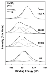
Oxygen 1s X-ray photoelectron spectroscopy data from HafSOx films annealed to a range of temperatures to monitor dehydration of the inorganic resist is displayed on the right.
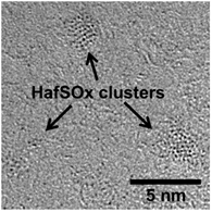
 High-resolution transmission electron microscopy images showing HafSOx clusters that makeup a baseline inorganic resist. |
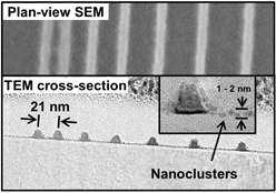
 Scanning electron and transmission electron microscopy images of nanopatterned HafSOx inorganic resists. |